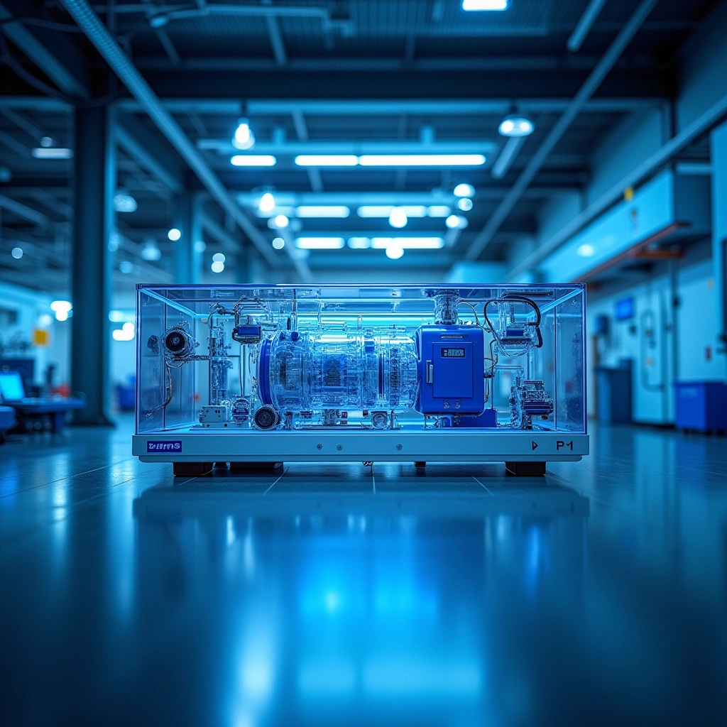
If you’re not familiar with the high-stakes world of semiconductor manufacturing, buckle up, because we’re about to dive into a topic that’s as exciting as watching paint dry—except, in this case, the paint is actually cutting-edge technology that powers everything from your smartphone to advanced AI systems. And yes, I’m talking about EUV (Extreme Ultraviolet) lithography scanners, specifically those produced by ASML, with a little help from their friends at Zeiss.
The High-NA-EUV lithography is the further development of EUV lithography. The higher numerical aperture allows structures with less than ten nanometers to be imaged on the microchip. With that, Moore’s Law will continue beyond 2030.
Recently, Zeiss made headlines by expanding its German site in Oberkochen, which is a name that sounds more like a fancy German beer than a hub for high-tech manufacturing. This expansion comes four years after the groundbreaking ceremony, which means they’ve probably had enough time to figure out how to brew that beer while also constructing a building that’s crucial for the production of EUV scanners.
Now, you might wonder, why is this expansion such a big deal? Well, for starters, ASML’s EUV scanners are the backbone of modern chip manufacturing. They essentially use light to carve out incredibly tiny patterns on silicon wafers. And when I say tiny, I mean so small that you’d need a microscope just to see them. If ASML is the wizard of chip-making, then Zeiss is the trusty wand supplier. Without Zeiss’s optics, ASML’s scanners wouldn’t even make it to the wizarding school.
So, what’s happening at this Oberkochen site? The new building is set to ramp up production capacity for the optical components that are vital for these EUV machines. You see, while ASML might be the star of the show, Zeiss is the unsung hero, quietly making sure that the scanners can actually do their job. Think of it like the backstage crew at a concert; without them, the whole performance would just be a bunch of confused musicians staring at each other.
The timing of this expansion is also noteworthy. With the global demand for chips skyrocketing—thanks to everything from electric vehicles to smart refrigerators (yes, those exist)—the pressure is on to produce more and more advanced chips. It’s like a never-ending game of Whac-A-Mole, where every time you think you’ve got a grip on supply, another demand pops up. Zeiss’s expansion aims to help ASML keep up with this relentless demand, ensuring that the semiconductor industry doesn’t come to a grinding halt.
Moreover, this expansion signifies a commitment to innovation and growth in the German tech sector. It’s a clear indication that Germany is not just about beer, pretzels, and lederhosen; it’s also a key player in the global tech arena. So, the next time you’re enjoying a nice stein of lager, remember that behind the scenes, people in Oberkochen are working hard to ensure that your devices can keep up with your binge-watching habits.
In conclusion, Zeiss’s new building in Oberkochen is more than just a construction project; it’s a vital step towards bolstering the production of EUV technology that powers our digital lives. And while it may not be the most exciting news to some, in the semiconductor world, it’s like a blockbuster sequel that everyone has been waiting for. So here’s to Zeiss, ASML, and the future of chip manufacturing—may it be bright, efficient, and free from supply chain hiccups (fingers crossed)!
Inspired by: “Zeiss expands German site that caps ASML’s EUV scanner output — first new building opens four years…” (r/technology)